3D integrated electronic devices and plasmon components have made important breakthroughs
February 23 10:20:50, 2021
[ China Instrumentation Network Instrument Development ] In 2015, the International Semiconductor Technology Development Roadmap (ITRS) Committee announced that Moore's Law is coming to an end, and the demand for silicon-based complementary metal oxide semiconductor (CMOS) technology is increasing. Among the many technical proposals, optoelectronic integration has the characteristics of high bandwidth and low transmission delay, and 3D integration has the potential advantage of increasing integration density and energy efficiency. Therefore, the three-dimensional optoelectronic integrated structure can combine the highlights of optoelectronic integration and three-dimensional integration. However, due to the incompatibility of materials and processing methods, it is difficult to integrate electronic and photonic devices in a three-dimensional form with the same feature size based on conventional materials.
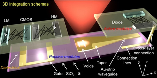
3D integrated architecture diagram
Emerging low-dimensional semiconductor materials (such as carbon nanotubes and two-dimensional materials) are potentially ideal electronic and optoelectronic materials that can meet the needs of three-dimensional optoelectronic integration in the film. On the other hand, plasmons have excellent performance in sub-wavelength size light control, which can solve the problem of incompatibility between electronic devices and photonics device features, so it has attracted attention in the field of sub-wavelength optoelectronic integration.
Professor Peng Lingmao, Key Laboratory of Nanodevice Physics and Chemistry, Department of Information Science and Technology, Peking University, proposed to use the "metal engineering" strategy to design a hole-like underlying plasmon structure based on gold (Au). In the light control. At the same time, since the gold film has nanometer-level flatness, it satisfies the requirement of constructing the top active device to the flatness of the substrate, thereby avoiding the mechanical polishing process and simplifying the preparation process. In the preparation of the plasmonic structure, all interconnect lines and electrostatic gate structures are prepared using gold. Since the low-dimensional semiconductor material has a thickness of an atomic layer size, the polarity of the device is not suitable for regulation by ion implantation. Therefore, it is an ideal choice to adjust the polarity of the device by adjusting the work function of the contact metal, that is, to realize the P-type metal oxide semiconductor by using different combinations of high work function (HM) and low work function (LM). PMOS) (HM-HM), N-type metal oxide semiconductor (NMOS) (LM-LM) and diode (LM-HM), enabling the use of low-temperature process technology and CMOS-compatible methods to achieve three-dimensional integrated plasmon Components and electronics. Its function is that the underlying passive components realize light control and signal transmission, and the upper active devices realize signal reception and processing. The following figure shows a receiver with unidirectional light control, a wavelength-polarization multiplexer and its 3D integrated loop with CMOS. The above integrated structure provides an important reference for the beyond the complementary metal oxide semiconductor architecture of the "Moore Age".
On December 13, 2018, the academic papers based on the above work were published online in Nature·Electronics with the title of “Three-dimensional integration of plasmonics and nanoelectronicsâ€. Nature Electronics). Liu Wei, a Ph.D. student at the Frontier Interdisciplinary Research Institute (now working as a postdoctoral researcher at the University of California, Los Angeles), is the first author and correspondent author of the paper. Peng Lianmao and Professor Zhang Jiasen from the School of Physics are co-authors. This is the first public report on the method of three-dimensional integrated electronic devices and plasmon components. Relevant work has been funded by the National Key Research and Development Program “Nano Research†and the National Natural Science Foundation.
(Original title: Peng Lingmao, School of Information, has made important breakthroughs in the research of 3D integrated electronic devices and plasmon components)